We design your power devices and ICs.
Please contact to: akio.nakagawa.dr@ieee.org
You can download and save the files by
clicking the right mouse button on the link.
[] I served as
Y. S. Sun Chaired Professor in Taiwan
National Tsing Hua University for 1 year stating Jan. 2015.
The
following is the lecture note of 6 hour presentation in the University.
"Basic
and Advanced Theory on Power Semiconductor Devices"
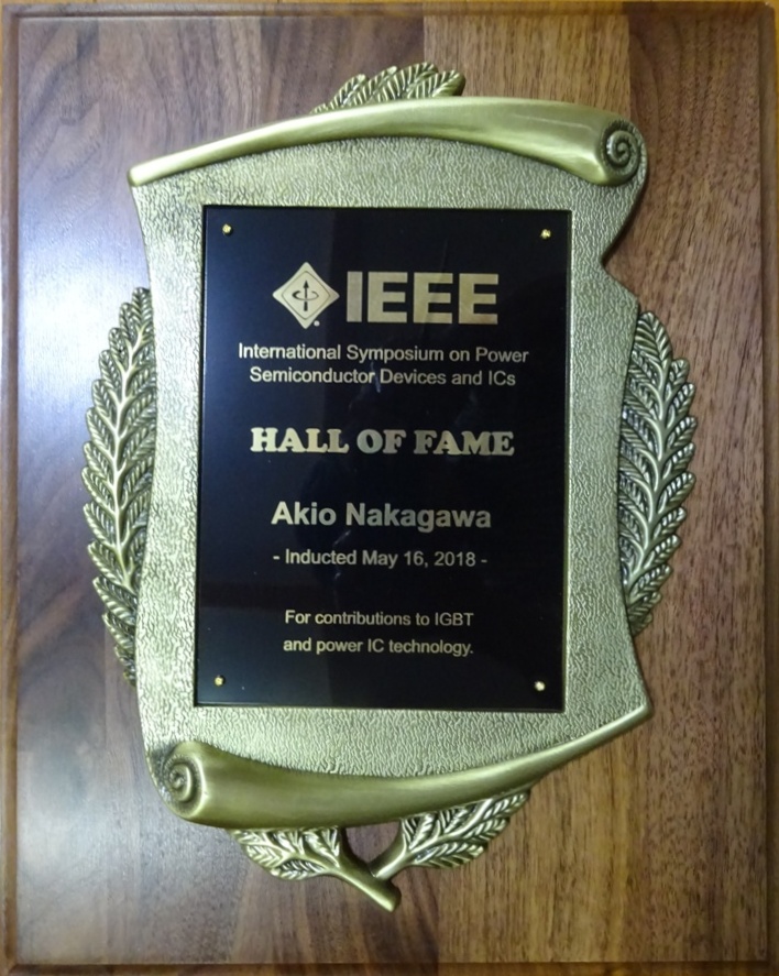
[] Selected as one of the inductees into the
ISPSD Hall of Fame in 2018.
[] Papers presented in ISPSD2018
Novel
3D Narrow Mesa-IGBT suppressing CIBL
IGBT
Structure with Electrically Separated Floating-p Region Improving Turn-on
dVak/dt Controllability
[] Papers presented in ISPSD2017
Conductivity
modulation in the channel inversion layer of very narrow mesa IGBT
Study
of the electrostatic potential of the floating-p region during the turn-on
period of IGBT
[] Papers presented in ISPSD2016
"Growth
of short-circuit current filament in MOSFET-Mode IGBTs"
[] Papers presented in ISPSD2015
"Simulation
Studies for Avalanche Induced Short-Circuit Current Crowding of
MOSFET-Mode IGBT"
"Investigation
of Anode-Side Temperature Effect in 1200V FWD Cosmic Ray Failure"
[] Papers presented in ISPSD2014
"Simulation
studies for short-circuit current crowding of MOSFET-Mode IGBT"を発表しました。
[] Papers presented in ISPSD2012
"Carrier-Storage
Effect and Extraction-Enhanced Lateral IGBT( E2LIGBT ): A Super-High Speed
and Low On-state Voltage LIGBT Superior to LDMOSFET"
"Analysis
for Rapid Tail Current Decay in IGBTs with Low Dose p-Emitter"
[]Development story of early stage IGBTs is presented here: 
[] Presentation file in the meeting
organized by IEEE Tokyo branch in January 17, 2012.
「世界を動かすシリコンパワー半導体−−その発展の経緯と未来」
[] Technical report on
SOI High Speed Diode published in the January issue of the Journal of the
Institute of Electrical Engineers of
Japan
(IEEJ Transactions on Industry Applications)
Authors : Norihito Tokyura, Takao Yamamoto, Hisato
Kato, and Akio Nakagawa
「横型SOI高速ダイオードの逆回復動作におけるダイナミックアバランシェ現象の解析と、その抑制構造の開発」 IEEJ
Trans. IA, Vol.132, No.1, 2012
[] In
SSDM2011 meeting of September 2011, we presented ultra-high speed lateral
IGBT superior to lateral DMOS.
Authors: Youichi Ashida,
Shigeki Takahashi, Satoshi Shiraki, Norihito Tokura, and Akio
Nakagawa,
“Extraction enhanced
lateral IGBT (E2 LIGBT) : A super high speed LIGBT superior to LDMOS”
[] Please look at this paper regarding the Silicon Limit of Power devices.
Akio Nakagawa, Yusuke
Kawaguchi and Kazutoshi Nakamura,
“Silicon Limit
Electrical Characteristics of Power Devices and ICs”, Proc. ISPS2008
[] Paper on High speed SOI Diode published in the associated meeting of the
Institute of electrical engineers of
「横型SOI高速ダイオードの逆回復動作におけるダイナミックアバランシェ現象の解析とその抑制構造の検討」
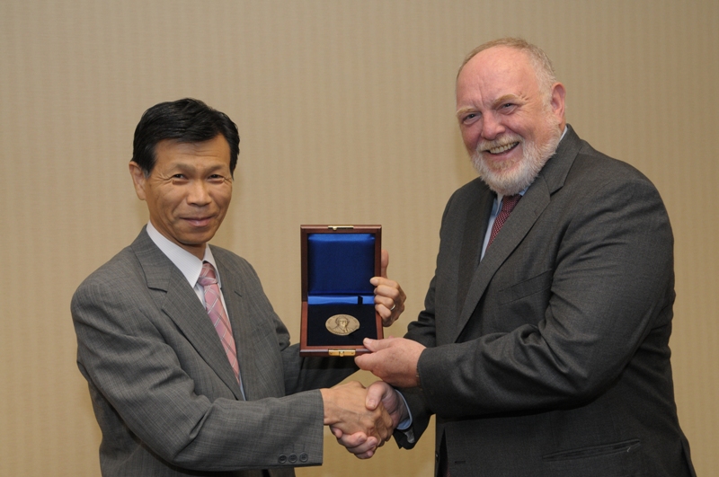
[] Received IEEE William E. Newell Power Electronics
Award, September, 2010.
Introduction of IEEE AWARD http://www.ieee.org/about/awards/bios/newell_recipients.html
Akio Nakagawa’s development of the non-latch-up insulated-gate
bipolar transistor (IGBT), which switches power at high speed, created an
indispensable power device now used in applications ranging from air
conditioners to hybrid vehicles. Before Dr. Nakagawa’s pioneering work in 1984,
IGBTs of that time were prone to failure or even destruction due to latch-up (a
type of short circuit) caused by the parasitic thyristor of the IGBT. His
invented design principles completely suppressed the latch-up even under
high-voltage and large-current operating conditions. The ability to withstand the
“load-short-circuit” condition for more than 20 µs exceeded the capability of
existing bipolar transistors. This set the global standard for IGBT design and
enabled its successful commercialization.
An IEEE Senior Member, Dr. Nakagawa is currently Technical Consultant of
Nakagawa Consulting Office. He previously served as Chief Fellow of Toshiba
Corporation Semiconductor Company,
[]
Presentation in
“History of power device development and the future technology” File1
“Power IC technology for supporting the ecological society―-High voltage
SOI and Low voltage BCD”
File1、File2
[]
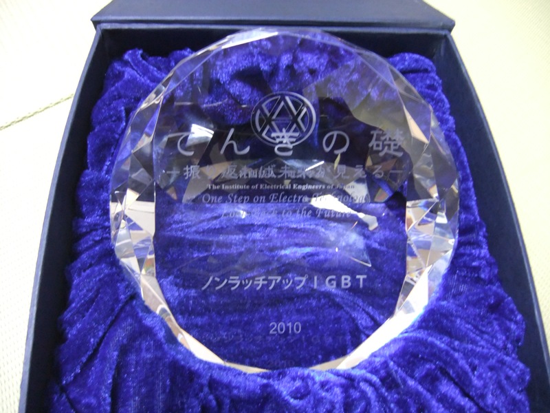
Non-Latch-Up IGBT selected as “One
step on Electro-Technology” of the Institute of electrical
engineers of Japan
in March 2010.
Introduction of “One step on Electro-Technology”→(http://www2.iee.or.jp/ver2/honbu/30-foundation/data07/3rd01.php)
・published「世界を動かすパワー半導体」in December 2012 by the Institute of
electrical engineers of Japan.
Independent
Consultant Akio Nakagawa
EXPERIENCE:
2009-present Nakagawa
Consulting Office, LLC.
Consultant
2005-2009
Toshiba Corporation, Semiconductor
Company,
Chief Fellow,
1999-2005
Toshiba R & D Center, Advanced Device Laboratory, Senor Fellow
1994-1999
Toshiba R&D Center, Material and Devices
Lab., Chief Scientist,
1988-1994
Toshiba R&D Center, Electron Devices
Laboratory, Group Manager,
1987-1988
ToshibaR&D Center, Electron Devices
Laboratory, Senior Researcher,
Sep. 1981- Feb.1983
EDUCATION:
The
1. Bachelor of Science
Degree
1972
2. Master of Science
Degree
1974
3. Ph. Doctor Degree in Electrical
Engineering
1984
Dissertation:
「改善した一次元半導体素子モデルとその素子設計及び動作解析への応用」
ACHIEVEMENTS
Dr. Nakagawa with the
following achievements has made outstanding contributions to the development of
power devices/ICs and power semiconductor device simulators, and their
applications. In particular, based on his pioneering work in the development of
non-latch-up IGBTs, IGBTs have become one of the major indispensable power
devices in the field of power electronics.
For more than 35 years, Dr.
Nakagawa has achieved and conducted comprehensive development and research work
on power devices and ICs, including high-efficiency diodes, power MOSFETs,
IGBTs, high voltage SOI (Silicon on Insulator) power ICs, BCD (BiCMOS DMOS) power ICs, and lateral DMOSFETs. His work also
includes pioneering work in the development of versatile 2-dimensional power
semiconductor device simulators in the 1980s. He applied power semiconductor
device simulators to advancing the technologies of power devices and ICs. He
authored and coauthored 150 technical papers in international journals and
conference proceedings, including five invited papers in 1991, 1992, 1996, 2000
and 2006. He was granted 104 Japanese patents and over 190
During the early development stages of
IGBTs, the devices were easily destroyed by the so-called “latch-up” of the
parasitic thyristor, inherent in IGBTs. At the time, preventing the latch-up of
the parasitic thyristor seemed to be nearly impossible for all the researchers
and engineers. Dr. Nakagawa set out to develop non-latch-up IGBTs that would
displace high power bipolar transistors. His intention was largely unrecognized
until he published a paper entitled “Non-Latch-Up 1200V 75A Bipolar-Mode
MOSFETs with Large ASO” as a late news paper in the 1984 IEDM (International
Electron Devices Meeting). He invented the device design principle of “non-latch-up IGBTs”(US
Patent No.6025622) and succeeded in completely suppressing the action of the
parasitic thyristor. The developed non-latch-up IGBTs achieved the world's
first so-called “short-circuit-withstanding capability.” This capability was
considered a requisite for displacing existing bipolar transistors. In 1985,
Toshiba commercialized the world first non-latch-up IGBT modules. The concept
of the non-latch-up IGBT became the global industry standard and, now, “IGBT”
automatically means “non-latch-up IGBT.” Dr. Nakagawa was granted 11 Japanese
patents and 8
Dr. Nakagawa began his
pioneering contribution to the development of 2-dimensional power semiconductor device simulators
in the early1980s. At that time, there were no 2-dimensional semiconductor
device simulators able to analyze the electrical characteristics of power
devices operating at voltages exceeding 100V. In 1982, he published a paper
entitled "A time- and temperature- dependent simulation of the GTO turn-off
process" in IEDM and established the basic method of solving 2-dimensional
highly nonlinear two-carrier transport equations with Poisson’s equation,
guaranteeing the numerical convergence and its solution even under high
operating voltages. In 1990, he further expanded the capability of the
simulator, named “TONADDEII,” and merged the device simulator with a
simplified circuit simulator. From 1990 to1995, he conducted an IGBT design
team, intending to develop high voltage IGBTs. His team successfully established
the key concept of the “injection enhancement effect” in IGBTs, and verified
the concept by using the 2-dimensional device simulator “TONADDEII.” The
concept was published in the paper, “A 4500 V Injection Enhanced Insulated Gate
Bipolar Transistor (IGBT) Operating in a Mode Similar to a Thyristor” in
the1993 IEDM. The “injection enhancement effect” enabled the development of
4.5kV IGBTs at Toshiba and made a great contribution to the power electronics
industry by realizing IGBT-based inverters for traction systems. The device
simulator was also used as a basis of the concept of high voltage SOI power
ICs, described in the next section. Dr. Nakagawa pioneered in the development
of the versatile power device simulator and its application to actual power
device design.
Dr. Nakagawa opened a new
field of high voltage SOI power IC
technology. He invented a new high voltage device structure,
making it possible to realize a 500V breakdown voltage device in only a 15-20um
(micrometer) thick silicon layer on buried oxide film. If the silicon layer was
thinner than 20um, it was easy to isolate the layer into island regions by deep
trenches. This realized dielectric isolation at reasonable cost.
Conventionally, a 50um thick silicon layer was required to achieve 500V and
trench isolation was impractical. Dr. Nakagawa thought of this new device
structure and verified its validity by using “TONADDEII.” He, then, made a
patent application in 1988 and was granted three
Dr. Nakagawa has also made a
great contributions to the advancement of low-voltage power IC technology,
so-called BCD power ICs, integrating lateral DMOS with BiCMOS
circuits. One of the problems in the lateral DMOS was that the on-state
breakdown voltage decreased as the current density increased. He conducted the
project team of BCD power IC development and, in 1998, the team invented the
concept of “adaptive resurf,” which
successfully prevented the reduction of on-state breakdown voltage even under
high current conduction. This invention enabled the adoption of BCD power ICs
for various application fields, especially, the automotive industry, and
greatly expanded Toshiba’s annual sales of BCD power ICs, which reached 15
billion yen in 2006. He and his team members were granted
Over the past 35 years, Dr. Nakagawa has
made truly extraordinary and sustained original and practical contributions in
the field of power semiconductor devices/ICs and also to power electronics
industry.
PUBLICATIONS:
1. Published 50 head author
papers in technical Journals and international conference proceedings.
2. Published more than 90
technical papers in technical Journals and international conference proceedings
as a co-author.
3. Published three books written
in Japanese as a co-author.
4. Published as a co-author “THE
VLSI HANDBOOK” edited by Wai-Kai Chen, CRC PRESS, ISBN 0-8493-8593-8
ACTIVITIES:
1. From 1997 to 1999, Chaired
Technology Survey Committee of “High performance and Intelligent Power
Devices/ICs” under IEE Japan.
2. Organized workshops in two
international conferences of ISPSD’01 and ISPSD’02.
3. Chaired Technical Program
Committee of ISPSD’04.
4. Served as members of various
program committees of IEDM, ISPSD, BCTM and PESC.
5. A member of extended steering
committee of JSPS University-Industry Research Cooperation 173rd
Committee.
6. A member of the Institute of
Electrical Engineers of Japan, and IEEE.
7. Granted over 100 Japanese
patents and over 190
AWARDS:
1. Received Okochi
Memorial Technology Prize in 1990 for the development of high voltage power
IGBTs
2. Received Toshiba President
Award in 1997 for the development of IGBTs
3. Received ISPSD Award in 1998
for his pioneering work in high voltage SOI technology.
4. Received Kanto-Region
Governor Invention Award for development of non-latch-up IGBTs
5. Received
two of Kanto-Region incentive invention awards.
6. Received Leadership Award for
outstanding achievement in the advancement of SEMI standard in 2000
7. Received Kanto-Region
incentive invention award for the invention of “Adaptive Resurf”
in 2005
8. Received IEEE WILLIAM E.
NEWELL POWER ELECTRONICS AWARD in 2010.